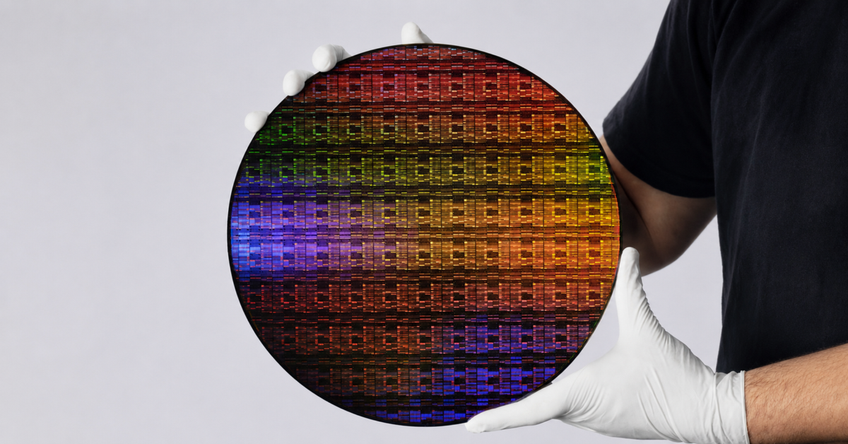
When IBM showed off its 2nm chip back in 2021, it felt like one of those moments that hinted at the future. Now the company has done it again, announcing what it says is the world’s first sub-1 nanometer semiconductor technology. If its research eventually reaches production, this could shape computing for years to come.
The new 0.7nm, or 7 angstrom, technology packs nearly 100 billion transistors onto a chip about the size of a fingernail. According to IBM, that’s nearly double the transistor density of its previous 2nm design. Even more impressive are the projected gains: up to 50 percent better performance or as much as 70 percent greater energy efficiency.
Those numbers are still based on research results rather than shipping products, but they paint an exciting picture for AI, cloud computing, smartphones, laptops, and just about every other device that relies on increasingly powerful silicon.
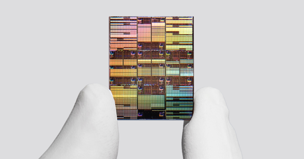
The real story, however, isn’t simply making transistors smaller. IBM says it achieved this milestone with an entirely new three-dimensional transistor architecture called “nanostack.” Rather than continuing to squeeze everything onto a flat surface, nanostack stacks transistors vertically and combines different materials within those layers to improve both performance and efficiency. It’s a reminder that the future of chip design isn’t just about shrinking features. It’s about rethinking how chips are built altogether.
IBM also says the technology could extend semiconductor scaling for at least another decade. That’s a bold claim, especially as the industry continues to wrestle with the physical limits of traditional manufacturing. Still, IBM has earned the benefit of the doubt. The company has a long history of semiconductor breakthroughs that later influenced the broader industry.
There’s another reason this announcement matters. For years, people have wondered whether Moore’s Law was effectively dead. IBM’s research suggests there may still be plenty of room for innovation, even if that innovation comes from entirely new architectures instead of conventional scaling.
Of course, don’t expect to buy a PC with one of these chips next year. IBM believes the earliest commercial adoption could happen within the next five years, assuming manufacturing challenges are overcome.
It’s easy to become cynical about announcements that promise to change the world. This isn’t one of those times, folks. IBM continues to prove that it remains one of the semiconductor industry’s true innovators. While companies like NVIDIA, AMD, Intel, Apple, and Qualcomm often grab the headlines with finished products, IBM keeps pushing the science forward behind the scenes. If nanostack lives up to its promise, today’s announcement could be remembered as one of the most important chip breakthroughs of the decade.
Support independent tech journalism
NERDS.xyz is independently owned and operated. If you enjoy my coverage of Linux, AI, hardware, cybersecurity, and tech culture, consider supporting the site on Ko-fi.
Support NERDS.xyz