
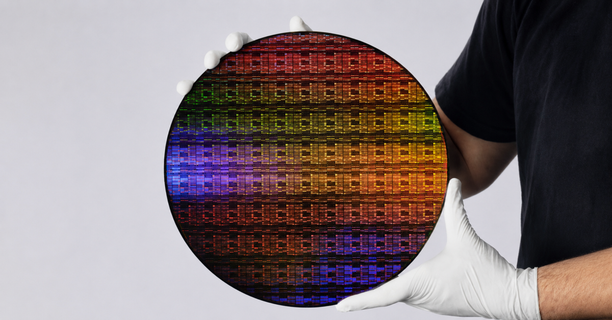
IBM has announced what it calls the world’s first sub-1 nanometer chip technology. The work is a research demonstration, not a processor headed to stores, but it shows one possible path for extending semiconductor scaling.
IBM describes the technology as a 0.7nm, or 7 angstrom, node with nearly 100 billion transistors on a chip about the size of a fingernail. The company says that is nearly twice the density of its 2nm design and projects up to 50 percent better performance or 70 percent greater energy efficiency.
Those figures compare research nodes, not finished consumer products. Manufacturing yield, power targets, cost, packaging, and chip design will determine how much of the projected improvement reaches commercial hardware.
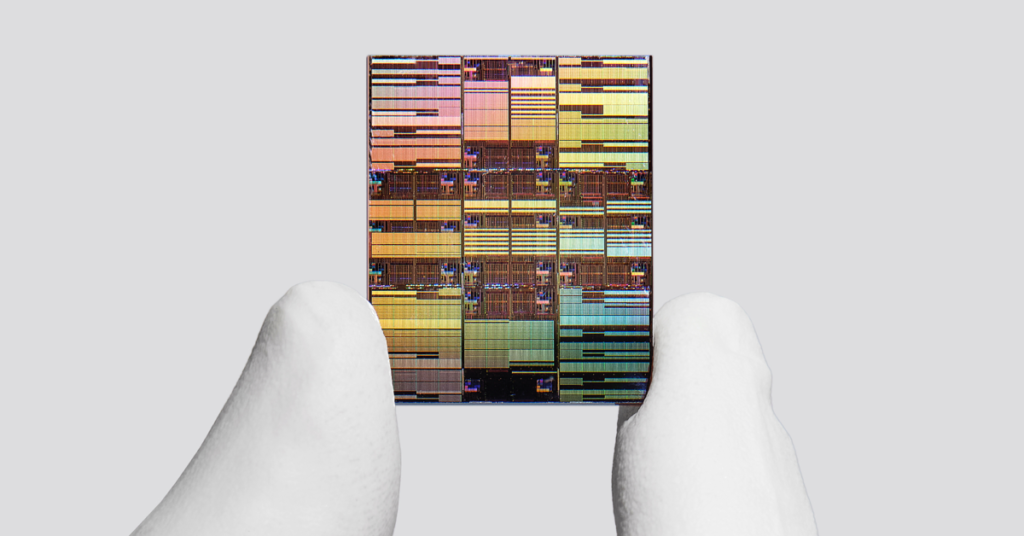
The important part is IBM’s three-dimensional transistor architecture, called “nanostack.” Instead of relying only on smaller features across a flat surface, the design stacks transistor structures vertically and combines materials within those layers. Also, 0.7nm is a process-node designation rather than the measurement of one physical feature across the chip.
IBM says nanostack could extend semiconductor scaling for at least another decade. That is an ambitious projection, and a laboratory demonstration cannot settle it. The value of the work will depend on whether manufacturers can produce the design reliably and affordably.
The announcement matters because conventional scaling faces physical and economic limits. IBM’s research suggests that new structures and materials may keep density and efficiency improving even when simply shrinking existing transistor designs is no longer enough.
IBM believes commercial adoption could begin within five years, assuming manufacturing challenges are solved. That timeline is the clearest limitation in the announcement. Readers interested in the production side can compare it with Apple’s U.S. chip manufacturing investment, which addresses capacity rather than transistor research.
Nanostack is worth watching, but IBM has not shown a shipping product, a production yield, or a commercial price. For now, this is credible semiconductor research with a long path between the laboratory and the devices people can buy.
Support independent tech journalism
NERDS.xyz is independently owned and operated. If you enjoy my coverage of Linux, AI, hardware, cybersecurity, and tech culture, consider supporting the site on Ko-fi.
Support NERDS.xyz